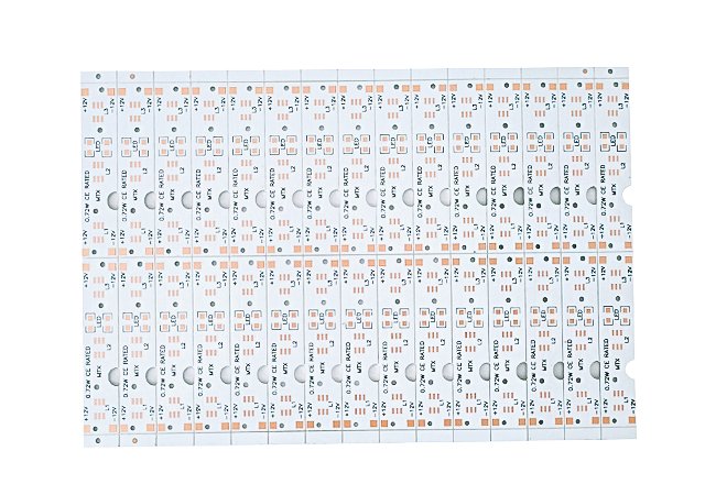
Metal base PCB process capability
| Biggest size: | 1190mm*490mm |
|---|---|
| Number of layers: | Single-sided AL-substrate, double-sided AL-substrate |
| Thermal Conductivity: | 1.0-2.0 |
| Minimum Trace Distance: | 8mil(0.2mm) |
| Drilling Hole Tolerance: | ±0.1mm |
| Minimum Trace Width | ≥10mil | Copper Thickness: | 18um/25um/35um/70um |
| PCB Thickness: | 0.8-2.0mm |
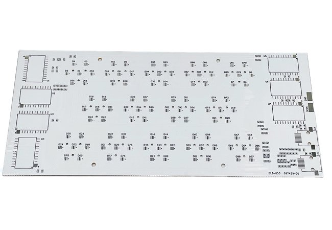
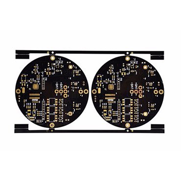
Metal-based PCB process
Aluminum substrate is a metal-based copper-clad laminate with good heat dissipation function. Generally, a single panel is composed of a three-layer structure, namely circuit layer (copper foil), insulation layer and metal base layer. For high-end use, there are also double-sided designs with a structure of circuit layer, insulation layer, aluminum base, insulation layer, and circuit layer. A very few applications are multi-layer boards, which can be made of ordinary multi-layer boards laminated with insulation layers and aluminum bases. After the circuit is laid out by software, the paths and holes are processed by printing, etching, machining, etc.
Many advantages of aluminum substrate PCB
Advanced surface mount technology (SMT) can be used in the assembly process
It can effectively reduce the operating temperature of the product and extend its service life;
Extremely effective handling of thermal diffusion in circuit design solutions
Replaces fragile ceramic substrates for better mechanical durability.
Features such as electromagnetic shielding and corrosion resistance
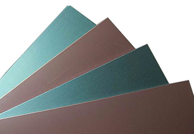
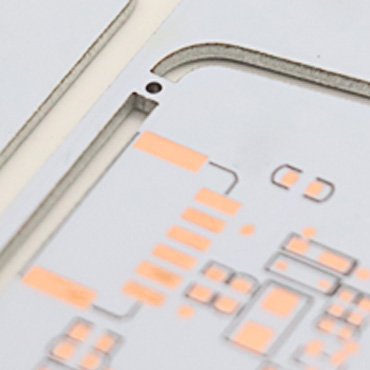
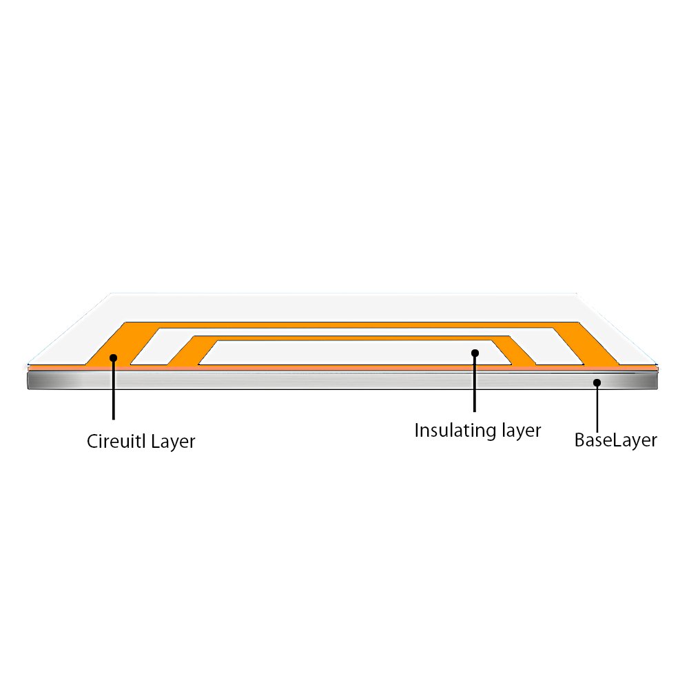
AL-PCB structure
Aluminum-based copper-clad laminate is a metal circuit board material, consisting of copper foil, thermal insulation layer and metal substrate. Its structure is divided into three layers:
Cireuitl.Layer circuit layer: equivalent to the copper-clad laminate of ordinary PCB, the thickness of the circuit copper foil is loz to 10oz.
DiELcctricLayer insulation layer: The insulation layer is a layer of low thermal resistance thermally conductive insulating material.
BaseLayer base layer: It is a metal substrate, usually aluminum or optional copper. Aluminum-based copper-clad laminates and traditional epoxy glass cloth laminates, etc.
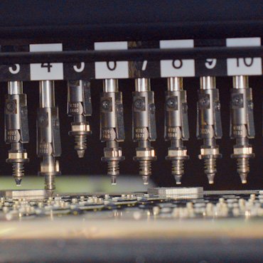
Process description
The circuit layer (i.e. copper foil) is usually etched to form a printed circuit to connect various parts of the component to each other. Generally, the circuit layer requires a large current carrying capacity, so a thicker copper foil should be used, with a thickness of generally 35μm~ 280μm; Thermal conductive insulation layer is the core technology of aluminum substrate. It is generally composed of special polymer filled with special ceramics. It has small thermal resistance, excellent viscoelastic properties, has the ability to resist thermal aging, and can withstand mechanical and thermal stress.
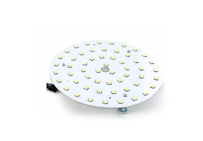
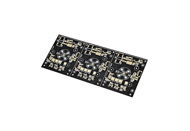
Application areas of aluminum substrates
Aluminum substrates are widely used in audio amplifiers, power conditioners on power supply equipment, energy-saving lamps and other fields in the electronics industry.