HDI PCB process capability
| Size: | Nigeria |
|---|---|
| Power: | 26000㎡ |
| Voltage: | Nigeria |
| Hertz: | 50Hz |
| Capacity: | 16P |
| Space Area: | 9m*9m |
| Speed: | up(2m/s)down(5m/s) |
| Configuration: | Double oil cylinder system |
HDI PCB process
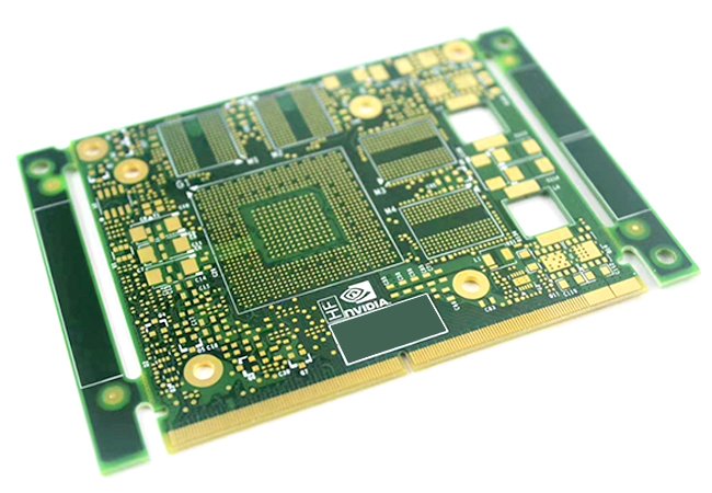
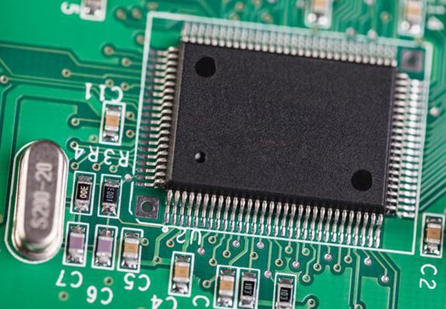
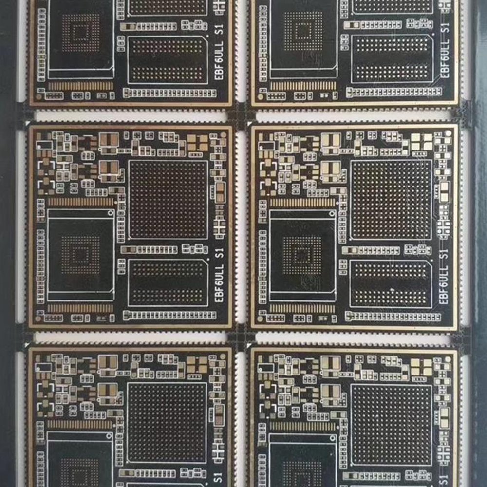
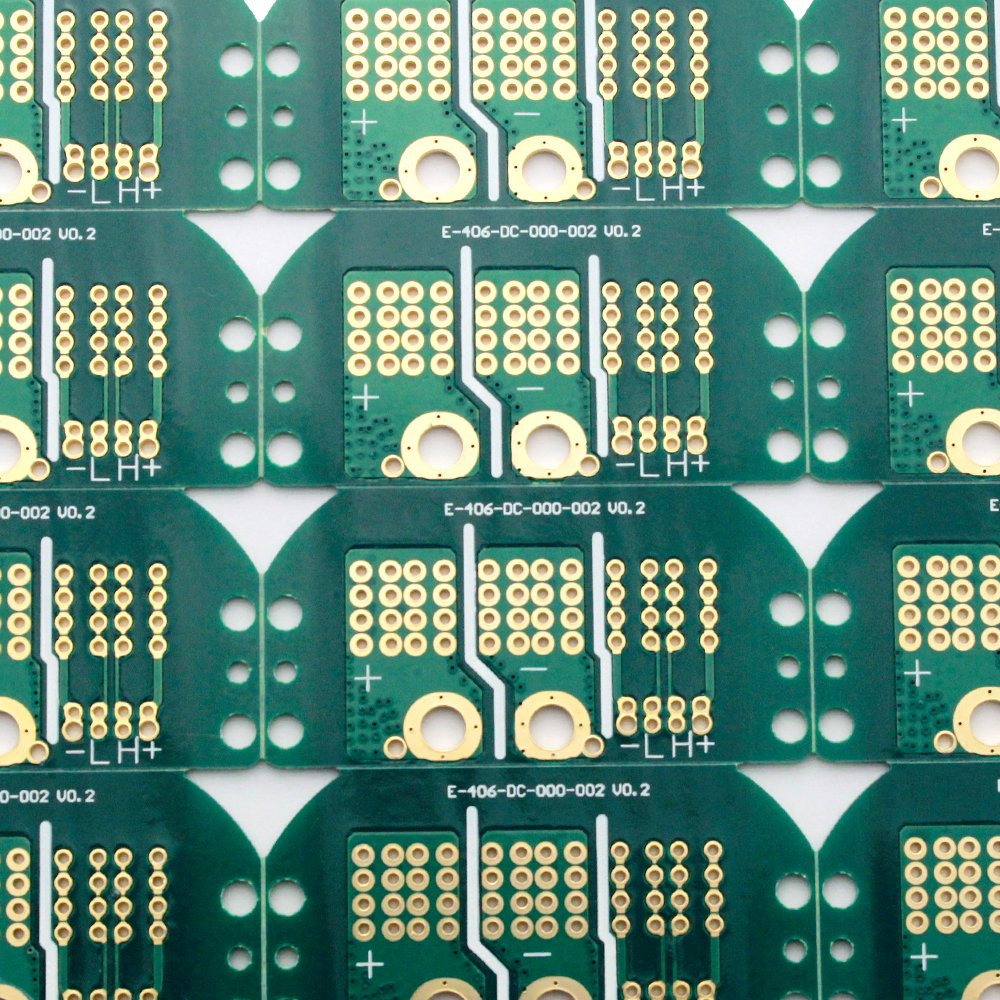
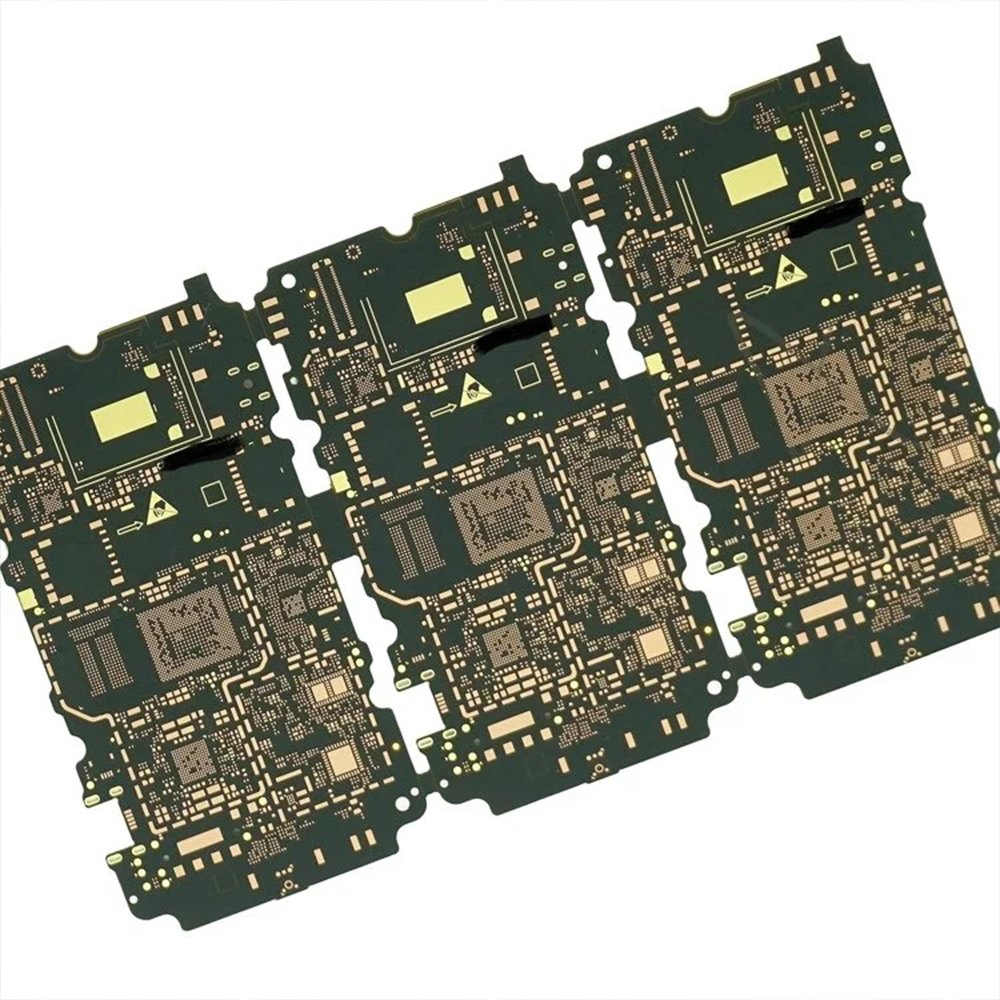
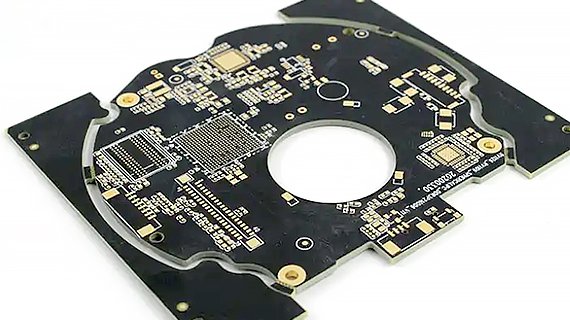
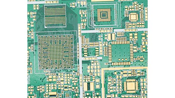
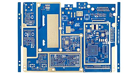
HDI PCB Is the abbreviation of high-density interconnection printed circuit board, is a printed circuit board manufacturing technology. HDI PCB Is a kind of circuit board with relatively high circuit density, using microblind embedded hole (i. e., copper plating hole in PCB) technology. China Dragon HDI PCB is a compact product designed for small capacity users. HDI PCB contains two types of blind holes and buried holes, and the circuit density is higher than traditional circuit boards. China Dragon HDI PCB Capable of making a HDI PCB of up to 38 layers.
Many advantages of HDI PCB
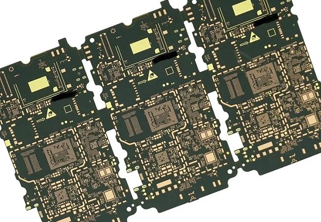
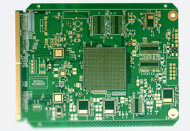
The HDI board uses more internal layers, which makes the connection between components more compact, improving the line density and signal transmission rate.
HDI PCB with higher circuit density and more complex circuit layout, it can achieve smaller size and thinner design requirements.
HDI PCB can achieve higher line density and provide more electronic device connection interface through the inner connection technology
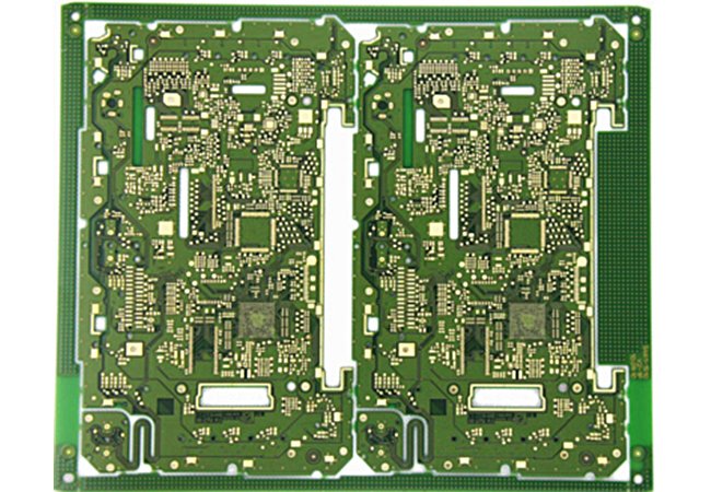
Because HDI boards can achieve smaller size and thinner design requirements, making electronic devices more portable and portable.
HDI pcb adopts blind holes and buried holes to reduce the signal transmission path and improve the transmission rate and stability of electrical signals
The complex design and fabrication process of the HDI board can improve the reliability and anti-interference ability of the circuit
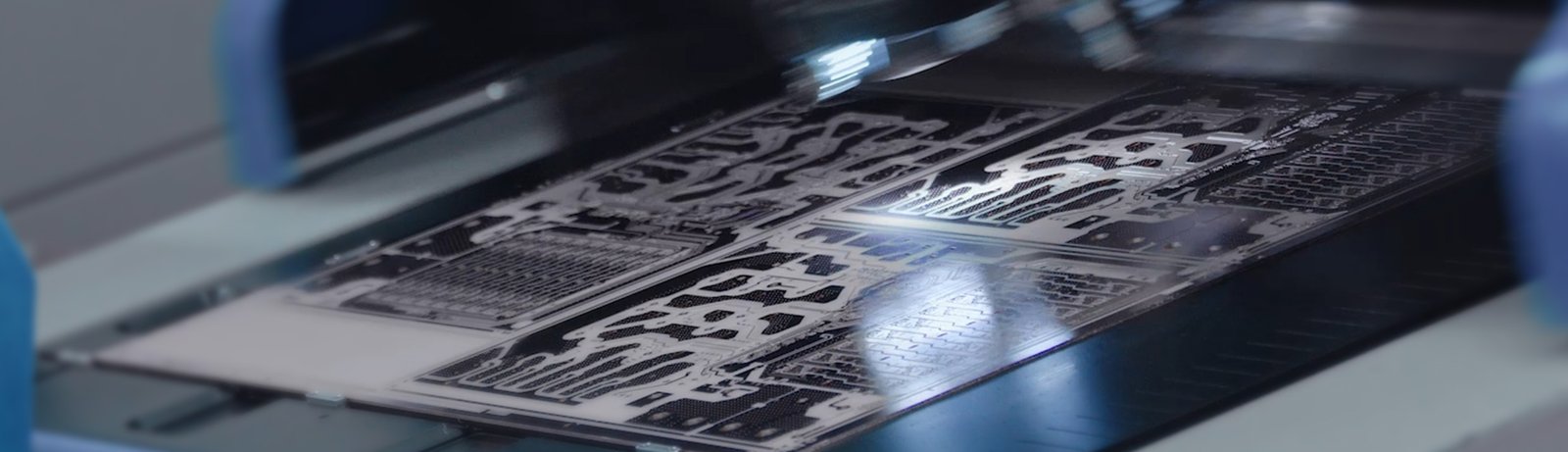
HDI PCB Manufacturing process
The complex design and fabrication process of the HDI board can improve the reliability and anti-interference ability of the circuit The manufacturing process of HDI plate is relatively complex, including laser hole (Laser Via), stacked copper plate, etching technology, etc., to achieve high density interinterconnection and complex circuit wiring. In contrast, the manufacturing process of ordinary PCB is relatively simple, generally using lithography, etching process, etc
HDI PCB Cost control
Because HDI board has more complex manufacturing process and has higher line density and technical requirements, its manufacturing cost is relatively high. Ordinary PCB has a lower manufacturing cost, which is suitable for some application scenarios with low line density and technical requirements. China Dragon Will give you a reliable, cheap HDI pcb
We have strict quality control
HDI PCB Compared with ordinary PCB, HDI board has higher line density and more complex circuit layout, making the difficulty of the finished product production process will be more difficult. China Dragon has nearly more than 20 testing equipment, which can fully ensure the production quality of each link.
HDI PCB Application field
HDI PCB are widely used in various electronic devices due to their unique advantages. The main application areas include, but are not limited to